
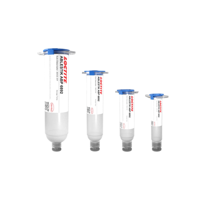
LOCTITE ABLESTIK ABP 6892
Harmonization Code : 3506.10.00.00 | Prepared glues and other prepared adhesives, not elsewhere specified or included; products suitable for use as glues or adhesives, put up for retail sale as glues or adhesives, not exceeding a net weight of 1 kg

Main features
- Designed for Fingerprint Sensors
- Low stress for ultra thin glass
- Low outgassing and finest filler
Product Description
LOCTITE ABLESTIK ABP 6892 is a transparent, non-conductive BMI/acrylate die attach adhesive developed for low-stress sensor assembly and applications requiring robust mechanical properties. It is used for fingerprint and optical sensor assemblies, including ultra-thin glass or ceramic bonding on sensor dies up to 10 x 10 mm. Its low modulus, low viscosity, fine filler size below 10 um, and improved flow support thin bond-line processing below 15 um. ABP 6892 also provides high optical transmittance, a refractive index of 1.50 with reflow-resistant optical performance, and minimal resin bleed-out, making it suitable for evaluation where optical performance and tight bond-line control are important.
LOCTITE ABLESTIK ABP 6892 has also been used for protection of Au wire-bond balls around the edge of a semiconductor die. In this application, the material was applied by jetting, where its flow characteristics and low-temperature, relatively short cure profile supported the production process. Its combination of fine filler, controlled flow, and transparent cured appearance can also support evaluation for localized wire-bond protection and optical encapsulation applications.
Key features
- Low-stress BMI/acrylate chemistry: Low-modulus cured behavior supports stress-sensitive sensor and thin-substrate assemblies.
- Fine filler for thin bond lines: Filler size below 10 um and improved flow support bond-line thicknesses below 15 um.
- Extended process window: 2-hour open time and 8-hour staging time, with a TDS work life of 24 hours at 25 C.
- Low-temperature cure option: Recommended cure includes a 15-minute ramp to 80 C followed by a 60-minute hold.
- High optical transmittance: Optical transmission remains high across the evaluated visible and near-infrared ranges, with performance dependent on wavelength, thickness, and thermal exposure.
- Reflow-resistant optical properties: Refractive index of 1.50 with minimal resin bleed-out supports optical sensor and precision-bonding applications.
- Environmental exposure performance: Robust adhesion and a void-free bond line were observed after 96 hours at 60 C/90% RH and 100 hours of HTS at 120 C under the evaluated conditions.
Applications / Suitable for
- Fingerprint and optical sensor assemblies
- Ultra-thin glass or ceramic sensor-die bonding
- Sensor dies up to 10 x 10 mm
- Thin bond-line applications below 15 um
- Au wire-bond ball protection using jet dispensing
- Optical encapsulation and localized sensor protection
ABLESTIK ABP6892
Unlike other products we offer, the products listed on this page cannot currently be ordered directly from the website.
 Shipping in 30 days
 Shipping in 12 weeks
 Shipping in 12 weeks
Technical Specifications
General Properties
Thermal Properties
Physical Properties
Additional Information
LOCTITE ABLESTIK ABP 6892
LOCTITE ABLESTIK ABP 6892 is a clear, non-conductive BMI/acrylate die attach paste developed for low-stress sensor assembly and applications requiring robust mechanical properties. The material is used for ultra-thin glass or ceramic bonding on sensor dies up to 10 x 10 mm and supports thin bond-line processing below 15 um. Its low modulus, low viscosity, fine filler size below 10 um, high optical transmittance, refractive index of 1.50 with reflow-resistant optical behavior, and minimal resin bleed-out support precision sensor and optical assembly applications.
ABP 6892 has also been used for localized protection of Au wire-bond balls around the perimeter of semiconductor die. Jet dispensing was used in this application, combining controlled material flow with a relatively low-temperature cure profile for production processing.
Material and handling properties
The clear paste combines low-viscosity processing behavior with thixotropy and an extended work-life window. Fine filler below 10 um supports flow into thin bond-line and localized encapsulation geometries.
| Property | Value | Unit | Method / condition |
|---|---|---|---|
| Technology | BMI/Acrylate | - | As supplied |
| Appearance | Clear paste | - | As supplied |
| Viscosity | 4,100 | mPa.s | Brookfield, 25 C, 0.5 rpm |
| Thixotropic index | 1.75 | - | Typical value |
| Work life | 24 | hours | 25 C |
| Shelf life | 365 | days | Stored at -40 C from date of manufacture |
Workability, thin bond lines and cure
ABP 6892 combines extended material work life with application-specific open and staging windows. Its fine filler and flow behavior support thin bond lines below 15 um, while two recommended heat-cure profiles provide processing flexibility.
Application window
Open time: 2 hours. Staging time: 8 hours. TDS work life: 24 hours at 25 C. These process windows should be treated separately.
Thin bond-line processing
Fine filler below 10 um and improved flow support thin bond-line assemblies below 15 um for ultra-thin glass, ceramic and sensor constructions.
80 C cure profile
Ramp for 15 minutes to 80 C, then hold for 60 minutes.
130 C cure profile
Ramp for 15 minutes to 130 C, then hold for 30 minutes.
Cure guidance: The cure profiles are guideline recommendations. Cure time and temperature may require adjustment for the application, curing equipment, oven loading and actual material temperature.
Thawing and dispensing controls
- Allow the container to reach room temperature before use.
- After removal from frozen storage, keep syringes standing vertically while thawing.
- Do not open the container until the contents reach 25 C. Remove any moisture from the exterior before opening.
- Do not re-freeze the adhesive after it has thawed to 25 C.
- Place thawed adhesive on dispense equipment for use. When transferring material to another reservoir, minimize air and contaminant entrapment.
- Use the adhesive within the applicable work-life window.
Low-modulus mechanical and thermal behavior
The cured adhesive has a glass transition temperature below room temperature and strongly temperature-dependent modulus. Tensile modulus is 176 MPa at 25 C, decreasing to 28 MPa at 100 C and 24 MPa at 150 C.
| Property | Value | Unit | Method / condition |
|---|---|---|---|
| Glass transition temperature | -24.6 | C | TMA |
| CTE below Tg | 111.4 | ppm/C | Below Tg |
| CTE above Tg | 190.6 | ppm/C | Above Tg |
| Moisture absorption | 0.44 | % | 85 C / 85% RH |
| Outgassing during cure | 0.7 | % | During cure |
| Thermal conductivity | 0.22 | W/mK | Test method not specified in supplied application data |
| Refractive index | 1.50 | - | Reflow-resistant optical behavior |
Temperature-dependent tensile modulus
| Test temperature | Tensile modulus | Unit | Method |
|---|---|---|---|
| -65 C | 1,912 | N/mm2 | DMTA |
| 25 C | 176 | N/mm2 | DMTA |
| 100 C | 28 | N/mm2 | DMTA |
| 150 C | 24 | N/mm2 | DMTA |
| 250 C | 34 | N/mm2 | DMTA |
Die shear on glass
| Test configuration | Temperature | Die shear |
|---|---|---|
| 3 x 3 mm Si die on glass | 25 C | 13 kg-f/die |
| 3 x 3 mm Si die on glass | 80 C | 6 kg-f/die |
These values are typical characterization data rather than guaranteed product specifications. Mechanical performance depends on the tested materials, bond-line geometry, cure condition, test temperature and assembly construction.
Transparent low-stress bonding and localized protection
Ultra-thin glass or ceramic bonding
ABP 6892 is positioned for transparent low-stress bonding of ultra-thin glass or ceramic on sensor dies up to 10 x 10 mm. Improved flow and fine filler below 10 um support bond-line thicknesses below 15 um.
Optical sensor and encapsulation evaluation
High optical transmittance, a refractive index of 1.50 with reflow-resistant behavior, low modulus and minimal resin bleed-out support evaluation where the cured adhesive lies within or close to an optical path.
Au wire-bond protection by jetting
ABP 6892 has been used to protect Au wire-bond balls around the edge of semiconductor die. Jet dispensing provided localized material placement while the low-temperature cure profile supported the associated production process.
Transmission across visible and infrared wavelengths
ABP 6892 has been characterized across both the visible/near-infrared region and an extended wavelength range to 2500 nm. The results show that optical performance depends on wavelength, adhesive thickness and thermal history, so application assessment should focus on the actual operating wavelength and expected bond-line thickness.
Visible transmission, thickness and thermal aging

Transmission from 800 to 2500 nm

Visible-spectrum
For specimens cured for 60 minutes at 80 C, transmission at 400 nm decreases from 95.73% at an actual thickness of 21 um to 94.89% at 55 um and 93.09% at 104 um. At 900 nm, the corresponding transmission values remain 100%, 99.88% and 99.84%. The thickness effect is therefore substantially more pronounced near 400 nm than at 900 nm.
Application implication: Bond-line thickness becomes particularly important when the optical system operates near the short-wavelength edge of the visible spectrum. A thinner and well-controlled adhesive layer can preserve more transmission around 400 nm, while applications operating closer to 900 nm are less sensitive to the thickness variation represented by this dataset.
Thermal-aging context: The thermal-aging curves use approximately 160 to 170 um thick specimens exposed for seven days at 85 C or 150 C. The higher-temperature exposure produces the larger shift of the short-wavelength transmission edge toward longer wavelengths. Because these specimens are substantially thicker than the 21 to 104 um thickness series, the aging curves should not be directly converted into quantitative predictions for a thin die-attach bond line.
Extended-spectrum
Transmission is generally high through portions of approximately 800 to 1600 nm, but it is not spectrally uniform. Distinct absorption regions appear around approximately 1200 nm, 1400 nm, 1700 to 1800 nm, 2100 nm and 2300 to 2450 nm.
Application implication: A transparent appearance or strong transmission at 850 to 940 nm does not establish equivalent transmission at every near-infrared or short-wave infrared wavelength. Optical sensor and emitter designs should therefore assess ABP 6892 at the specific wavelength used by the device, particularly when that wavelength is near one of the absorption regions.
Transmission by adhesive thickness
| Nominal thickness | Actual thickness | Transmission at 400 nm | Transmission at 900 nm |
|---|---|---|---|
| 15 um | 21 um | 95.73% | 100% |
| 50 um | 55 um | 94.89% | 99.88% |
| 100 um | 104 um | 93.09% | 99.84% |
Optical-data qualification: Optical performance depends on wavelength, material thickness, cure profile, thermal exposure and the complete optical path. The datasets above should be used for application evaluation under their stated test conditions rather than as guaranteed transmission specifications for other assembly configurations.
Dielectric constant and dissipation factor
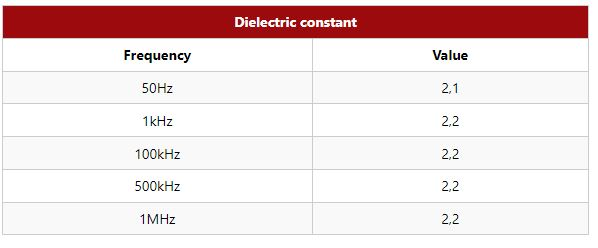
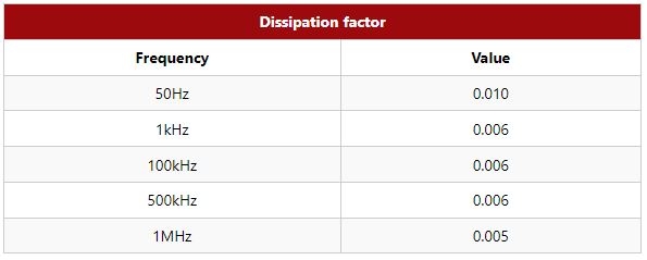
Dielectric constant remains between 2.1 and 2.2 across the supplied 50 Hz to 1 MHz dataset. Dissipation factor decreases from 0.010 at 50 Hz to 0.005 at 1 MHz.
| Frequency | Dielectric constant | Dissipation factor |
|---|---|---|
| 50 Hz | 2.1 | 0.010 |
| 1 kHz | 2.2 | 0.006 |
| 100 kHz | 2.2 | 0.006 |
| 500 kHz | 2.2 | 0.006 |
| 1 MHz | 2.2 | 0.005 |
Electrical-data limitation: The supplied dataset identifies frequency but does not provide specimen geometry, test temperature, cure condition, electrode configuration or measurement method. The values should not be extrapolated beyond the tested frequency range without additional validation.
Bond-line observations after humidity and thermal storage
ABP 6892 demonstrated robust adhesion and a void-free bond line after the two environmental exposures below. The observations apply to the evaluated construction and test conditions and should not be interpreted as universal package qualification.
Humidity exposure
60 C / 90% RH
Exposure duration: 96 hours. Robust adhesion and a void-free bond line were observed after exposure.
High-temperature storage
120 C HTS
Exposure duration: 100 hours. Robust adhesion and a void-free bond line were observed after exposure.
Performance data and application validation
Optical, dielectric, mechanical and environmental results on this page represent performance under specific specimen dimensions, materials, cure conditions, aging exposures, frequencies, wavelengths and test configurations. Actual performance can vary with bond-line thickness, substrate, surface preparation, package geometry, optical path, cure process, temperature, humidity and assembly design. Customers should validate ABP 6892 under their actual manufacturing process and qualification conditions before production use.
Evaluate ABP 6892 for your sensor or optical assembly
Krayden can support evaluation of ABP 6892 for bond-line thickness, sensor-die geometry, jet dispensing, optical wavelength, cure profile and environmental requirements. Contact us to discuss technical data, samples, processing considerations and qualification planning for your specific glass, ceramic, wire-bond or optical assembly.
Contact Us


